

Scope creep happens fast. A basic product quickly demands wireless connectivity, an interactive display, secure remote updates and a few more ‘what if?’ feature requests. For engineering teams under tight deadlines, the easy default is to either add a second chip or default to a complex Linux processor with additional memory peripherals just to manage the software burden. It feels like a safe, low-risk move in R&D, but it drives up Bill of Materials (BOM) costs, complicates the supply chain and doubles long-term firmware maintenance.
On a recent project, we took a bolder route: we ran everything through a single embedded microcontroller unit (MCU).
The false comfort of extra silicon
Product development rarely goes in a straight line. Features get added late, a complete board respin costs weeks or months, and a missed launch window costs far more. So when an existing product needs a new capability, the shortcut is to offload the new task to a second chip instead of reworking the hardware design. The same thinking applies to processor choice, where an expensive chip with plenty of headroom can absorb heavier calculations and processes, so the code doesn’t need to be as optimized.
The project looks safe in the short term, and that is exactly what makes these shortcuts so tempting. The cost shows up later on every unit shipped, as a more complex board, more components and a higher bill of materials (BOM).
Value engineering takes the opposite approach. Rather than just adding silicon, it analyzes the product architecture to remove cost, complexity and unnecessary components without losing function or quality. In practice, that means tight memory use, careful real-time scheduling and no extra silicon that isn’t pulling its weight.
Squeezing a multi-protocol system into one chip
We put value engineering to the test when a client asked us to integrate concurrent Bluetooth, Wi-Fi, Ethernet, NFC, and AirPrint into a high-performance label printer. Standard practice would have split the workload across two chips; one chip handles communication protocols on one side and real-time print control on the other.
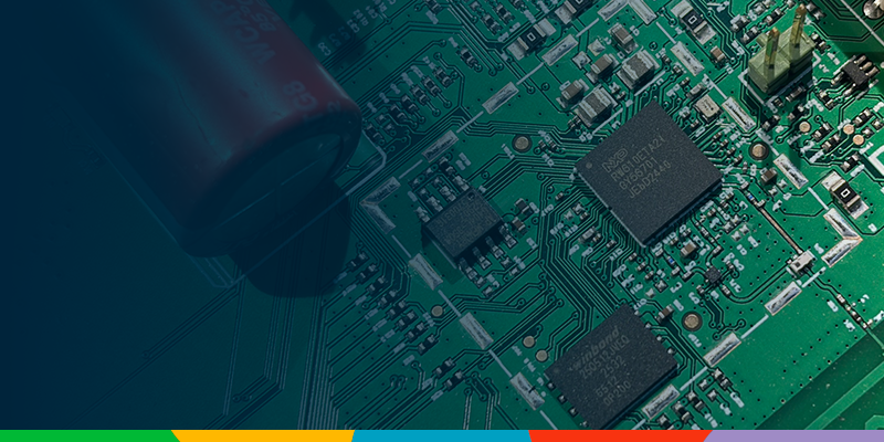
Instead of accepting multi-chip bloat or heavy inter-chip communication overhead, we built the whole system around a single NXP RW610 MCU. We ran all protocols concurrently and used the chip close to its full capacity.
- Connectivity & security: AirPrint (IPPS and mDNS) is supported over Wi-Fi, Ethernet and USB, alongside Bluetooth and NFC for label detection. Secured with a hardware root of trust, a tamper-resistant component built into the silicon.
- Deterministic real-time control: Maintained microsecond-precision timing for physical print head control.
- Maximized memory: Re-engineered memory allocation and system code to fit the complete stack into tight onboard storage.
Without the headroom of a second chip, every feature has to earn its place in memory and processing time. We managed that by setting a memory budget early and kept enough flash free for secure over-the-air (OTA) updates.
The single chip architecture passed our worst case stress test–handling all active interfaces while printing at maximum speed. And by building the firmware on Zephyr, we gained built-in OTA capabilities and a maintained security stack ready for the Cyber Resilience Act (CRA). That shows meeting modern cybersecurity requirements doesn’t call for overly complicated hardware and software.
Less silicon, better margins
The most direct win sits right on the balance sheet: eliminating the secondary processor saved 5 to 10 euros from the unit BOM cost. For a product shipping 100,000 units a year, that’s up to 1 million euros dropping straight back into your gross margins every year.
Getting there took real engineering effort. We took over the existing firmware, moved it onto the new MCU and integrated the communication stack alongside it, without disrupting the functionality the product already had. By not using an extra chip, we eliminated inter-processor communication bugs, dual bootloaders and the ongoing headache of managing dual-firmware updates. Everything now runs on one framework, with one unified codebase. The result is a system that is much easier to maintain.
Fewer components on the board also transform supply chain and field reliability. A leaner printed circuit board (PCB) minimizes vendor dependencies, protects production against component shortages and removes potential hardware failure points in the field.
Are you paying for hardware you don’t need?
Before you commit to a larger processor or add a secondary chip on your next board revision, ask your team: Are we really maximizing our silicon, or are we paying for extra hardware we don’t need?
At Verhaert Product Innovation, we bring deep R&D expertise and smart engineering together to optimize product architecture for maximum performance and profitability. Whether you are facing manufacturing cost challenges with an existing product or preparing a major redesign to protect your margins in production, we can help.
Reach out to explore how we can optimize your hardware design and cut your unit BOM costs!